
signal reflections in high-speed printed circuit boards
Mitigating signal reflections in high-speed printed circuit boards (PCBs) is crucial for maintaining signal integrity and ensuring reliable operation of electronic devices. Signal reflections occur when an electrical signal encounters an impedance mismatch along the transmission path, leading to partial signal energy being reflected back towards the source. These reflections can cause signal distortion, degradation, and timing errors, impacting the performance and reliability of high-speed digital and high-frequency analog circuits. Several techniques can be employed to mitigate signal reflections and optimize signal integrity in high-speed PCB designs.
One effective approach to mitigating signal reflections in high-speed PCBs is through proper impedance matching of signal traces. Impedance matching involves adjusting the electrical impedance of the transmission line to match the impedance of the connected components or transmission medium, minimizing signal reflections at the interface. By carefully controlling trace geometry, dielectric properties, and termination techniques, designers can achieve accurate impedance matching and reduce the risk of signal reflections in high-speed PCB designs.
Moreover, controlled impedance routing techniques can help minimize signal reflections and maintain consistent impedance along signal traces in high-speed printed circuit board. Controlled impedance routing involves fabricating PCB traces with precise dimensions and impedance profiles to ensure uniform signal propagation characteristics. By controlling trace width, thickness, and spacing, designers can achieve the desired characteristic impedance and minimize impedance variations along the transmission path, reducing the likelihood of signal reflections and preserving signal integrity.
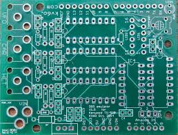
how do you mitigate signal reflections in high-speed printed circuit boards?
Furthermore, impedance discontinuities such as stubs, vias, or impedance transformers can be strategically used to mitigate signal reflections in high-speed PCBs. Stub matching involves adding short, controlled-length stubs to the signal trace at specific intervals to adjust the effective electrical length and impedance of the trace, minimizing reflections at the end of the transmission line. Vias can be used to transition between different impedance traces or layers, providing impedance continuity and reducing signal reflections. Additionally, impedance transformers such as tapered traces or transmission line transitions can be employed to match impedance between traces with different characteristic impedances, minimizing reflections at transition points.
Additionally, termination techniques can be employed to absorb reflected signals and improve impedance matching at the receiving end of signal traces in high-speed PCBs. Termination resistors or termination networks can be added to the receiving end of the transmission line to match the impedance of the load and absorb reflected signals, preventing signal reflections from propagating back along the transmission path. Common termination techniques include series termination, parallel termination, and termination using termination resistors or termination networks, each offering different advantages in terms of signal integrity and performance.
Moreover, careful signal routing and layout optimization can help mitigate signal reflections in high-speed PCB designs. Signal traces should be routed with proper spacing, routing topologies, and signal paths to minimize impedance variations, discontinuities, and coupling effects that can lead to signal reflections. Differential signaling can also be employed to improve noise immunity and reduce signal reflections by transmitting signals as a pair of complementary signals with equal and opposite voltages.
Furthermore, simulation and modeling tools can be used to analyze signal reflections and optimize PCB designs for signal integrity. Advanced simulation software, such as electromagnetic field solvers and signal integrity analysis tools, allows designers to model signal propagation, impedance matching techniques, and termination strategies and evaluate their impact on signal integrity. By simulating signal behavior under various conditions and analyzing simulation results, designers can identify potential sources of signal reflections and implement effective mitigation strategies to optimize signal integrity in high-speed PCB designs.
In conclusion, mitigating signal reflections in high-speed printed circuit boards (PCBs) is essential for ensuring reliable operation and optimal performance of electronic devices. By employing techniques such as impedance matching, controlled impedance routing, impedance discontinuities, termination, careful signal routing, and simulation-based optimization, designers can minimize signal reflections and preserve signal integrity in high-speed PCB designs. Through careful planning, design optimization, and adherence to best practices in signal integrity, designers can achieve superior performance and reliability in high-speed electronic systems and meet the demanding requirements of modern electronic applications.


